In the tuning world if you decide that you would like to keep the stock ECU and just adjust the maps contained within then this is the guide for you. My neighbor needed this done so today we are going to chip a Honda ECU, P28 or similar. The basic skills of this really apply toward chipping any ECU that just lacks a few components, the other main intent of this guide is to outline some help de-soldering techniques.
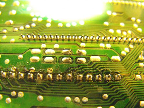
So lets take a look at our ECU, with this specific computer the area that needs components inserted into it is actually surrounded in a dashed white line, interesting convenience. The 27C256 outline below is the “EPROM” which will actually contain the maps. This is the chip that you “burn”, the other chip “74HC373” acts as an “interface” between the EPROM and the processor inside the ECU. Notice how all the pads are filled with solder to lets goto work exposing the holes:
Looking at the below picture just the left of center you’ll see a group of 4 rectangular pads and 2 more off the right that are flat in comparison to the pads in the very center of the picture, these are the holes that we will use as an example (note the completed added chip socket pads make up the row just below)
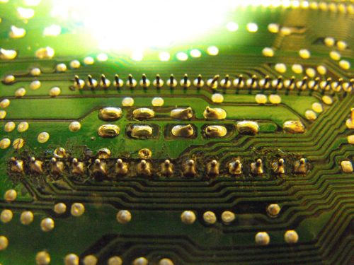
Next I tinned every pad that needs to be de-soldered, adding a little bit of new solder to make the overall process easier. I have noticed that old pads will be significantly harder to clean up without tinning them in this way. I don’t even touch the solder to the pad I touch it to the top of the iron’s tip, the pad will instantly flash into an all liquid state, then you can move onto the next pad:
For the actual de-soldering part you’ll be needing some solder wick. This is basically a fine braided flat copper wire rolled onto a mini spool. Out of the brands I have used so far, pro wick has been the best. You’ll want to select the widest wick possible to suit your application, also when working with it keep in mind that copper transfers heat extremely well so you will want to keep your finger placed up the wire a bit so you don’t burn it. I always bend a 90 degree angle in it so the wick doesn’t flash or suck up the solder from neighboring components:

When actually de-soldering you’ll want to move up the wick about or at least 1/4 on an inch, or 10mm with every next pad you de-solder, and your soldering iron will need to be on a higher setting, I set my digitally controlled Weller somewhere around 750 – 800 degrees F (420* C). The reason for the spacing is the flux of the solder will spread out on either side of the heat point as the solder transfers to the wick, resulting in a reduced overall sponging capacity at close distances from the central de-solder point on the wick, so spacing yourself on the wick is critical. If you don’t suck up all the solder so the hole is clean through, grab your roll and re-tin the pad, move further down the wick (maybe a slightly greater distance than before.) and press and hold for approximately 5 seconds, you will be able to see the sponging action take place as it happens and if you keep an eye on the wick you can see why the spacing is needed. Not everyone is perfect not even me, I missed the first two holes because when I folded the end I started to close to the end (you’ll want to in-set 1/4 inch when starting from the solder wick end) and the subsequent attempt was also too close the 1st:
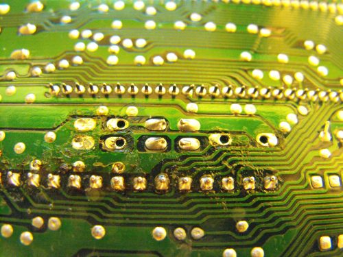
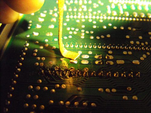
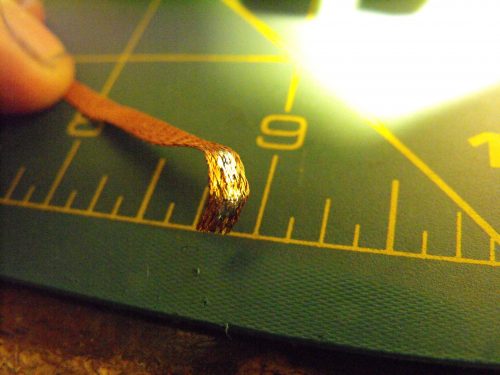
Here is the top of the solder wick so you can get a better idea of spacing / what it looks like goobered up:
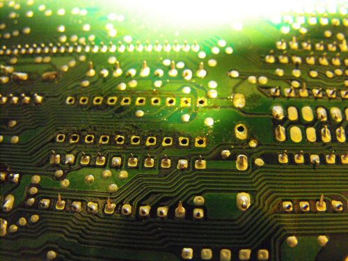
 Looking at the bottom side you can tell it’s a pretty continuous line of solder, remember that the thinner the wick the further you’ll need to expect to space out:
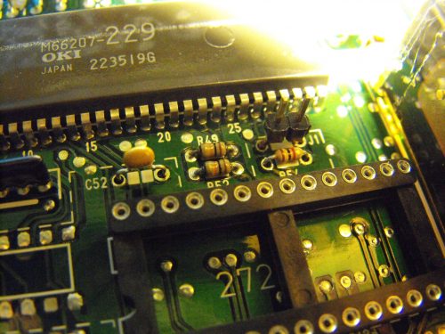
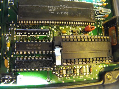
Here is a picture showing the components added into the holes we just cleared out, the two brown/black/orange resistors in the center make up the “center reference point” in the top picture:
Next I cleared the solder pads for the 74HC373, and it’s “noise capacitor” off to the right. Notice in this picture I only missed one hole, the other hole for the capacitor. Some good soldering tips to keep in mind is remember to regularly sponge your iron tip and tin appropriately. Remember to heat the surface that you are applying solder to before applying the solder rather than globbing it on the iron.
Here is the completed added in circuit, we are now ready to pop in our EEPROM with our custom maps and start tuning. All of this for the sweet sounds of boost:
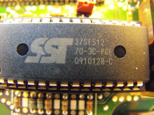
The type of chip used in this to store the maps is of the usual 27C eprom series flavor, we use the SST 27SF512. This is pin to pin compatible with the 27cxxx series eprom chips but this one is electrically eraseable because it contains flash memory. It’s compatible with the Willem prom burners for sure and I have had great success with this chip, so it comes highly recommended:
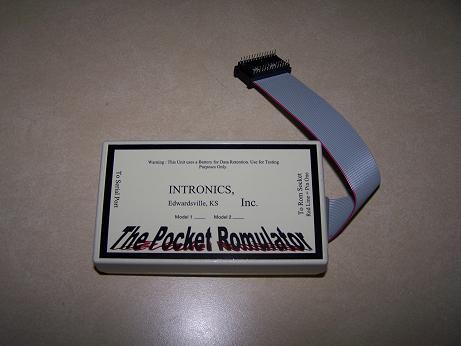
Chip tuning an ECU isn’t always as straight forward as it is on Honda ECU shown above. There are several different scenarios which can warrant the use of a daughter board. Sometimes they are needed in the form of a Romulator, which creates a real time tunable environment for the ecu by holding the entire contents of the EPROM in a ram and that is where the ECU reads it from, all while you’re plugged into a serial port on the board with your laptop adjusting the values with the car on a Dyno. If the ECU needs to deal with checksums in some cases you’ll need to shut down the engine to write the new data but its still much faster than burning and juggling chips. There are external types of ROM Emulators and then there are those that have been consolidated into a plugable, hideable board. Sometimes performance companies package this concept into their design and you get products like what Hondata offers.
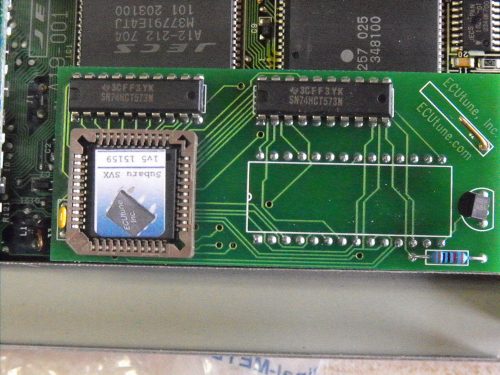
Sometimes a board is required when the issue at hand is more technical. The Subaru SVX ECU is a great example, actually many OBDI JECS ecu’s required a sort of “adapter board” to be able to adjust the ROM inside. The reason for this is because the JECS ECU’s use chips that have 16 address and data lines, but the two functions are multiplexed over the same set of wires. (Each pin is both an address and data line) Since programmers and proms of that style aren’t readily available or cost thousands of dollars a board adapting to a more economical solution is the best bet. In this case the JECS ecu I am modifying uses a 27c1028 Eprom, which isn’t available anymore. This adapter board pictured below converts the 27c1028 into a 16bit EPROM. This PROM not only had the 16 address and data lines, but it also is large enough in capacity that it can hold two separate maps. (The square chip pictured below) The other two chips that are off to the side will take the data output from the EPROM and retain it in a temporary memory until the ECU needs to read the next 16 bits of data:
This is a nice little production piece, but still not completely practical for the DIY user, since this utilizes a 16 bit EPROM you’ll need to find an adapter for your programmer to be able to use it. (I bought my programmer with a 16 bit adapter) There is however more than one way to a solution. A very nice man by the name of Phil developed an adapter board for the Subaru SVX and instead of using 1 16 bit EPROM it utilizes 2 8 bit PROMS and merges the two together (ODD and EVEN) to create a 16 bit data signal back to the ECU’s upgrade socket. These proms are extremely common and even come in a EEPROM from so there is no fuss with a window that you need to have a UV light to erase, it’s all done electrically. This information and just about everything you need to get started reverse engineering SVX and other JECS ECU’s can be found on his site: http://www.alcyone.org.uk/ssm/index.html There is much there to read and should take you a couple of weeks of reading and experimentation to grasp the fundamentals, and once you do have them you’ll be well on your way to not only tuning your car, but modifying other code and having a better understanding of how EFI works in it’s OEM implemented form. After ordering the board via the Express PCB software I received the boards in the mail about a week later and obtained the appropriate parts and assembled them:
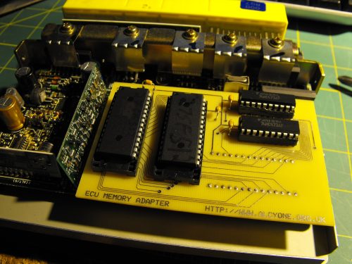
This is what I have been running in my car since, I bought some ZIF sockets that plug into the regular sockets for tuning purposes. It’s sure nice to not have to pry the chips out every time and when you’re done you can plug the chips into a more permanent home leaving ample room for the cover to go back on without the risk of shorting. They make shorter height ZIFs but at the time those options seemed to be a lower quality option.
That pretty much covers all your possible tuning options when working with a factory pre OBD-II ecu. If you have a car that is OBD-II (1995.5 or newer) you have the major convenience of not having to fuss with any of this stuff (usually) and you can make adjustments and upload new images via the diagnostic port. Of course there are some complications because of “security” measures implemented by each manufacturer.. (i.e. Checksums, and even encryption) These however can and have been sidestepped time and time again.
This guide was intended to be general, if you would like to see anything added on to it or have any questions please feel free to email me.


